
 1005 Alcyon Dr Bellmawr NJ 08031
Scientists are working to discover new semiconductor materials that can improve the efficiency of solar cells and other electronic products. However, the speed of innovation is through the speed bottleneck where researchers can manually measure the properties of important materials.
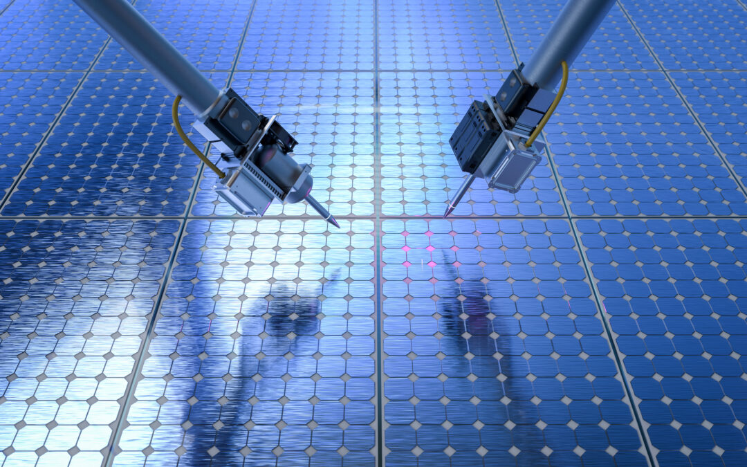
A fully autonomous robotic system developed by MIT researchers can speed up.
Their system uses robotic probes to measure important electrical properties called optoelectronic traditions, which is the way the material responds to the presence of light.
Researchers inject materials science domain knowledge into machine learning models that guide robotic decision-making. This allows the robot to determine the best location to contact the material with the probe to get the most information about its optoelectronic automation, while a professional planner finds the fastest way to move between contact points.
In the 24-hour test, the fully autonomous robot probe was performed with only measurements of more than 125 times per hour, with greater accuracy and reliability than other AI-based methods.
By greatly increasing the speed at which scientists can characterize important properties of new semiconductor materials, this approach can stimulate the development of solar panels that produce more electricity.
“I find this article very exciting because it provides a pathway for autonomous, contact-based characterization methods. Every important property of the material can be measured in a contactless manner. If you need to contact the sample, you want it to be fast and you want information about profitability,” Professors from Tonio Buonio buonio buonio buonio buonio buonio buonio buonsisi of Tonio buonio buonsisi of Mechanitial Engineering and Papers of Papers of Papers of Papers of Papers of Papers of Papers of Papers of Papers of Papers of Papers of Papers of Papers of Papers of Papers of Papers of Papers of Papers of Papers of Papers of Papers of Papers of Papers of Papers of Papers of Papers of Papers of Papers of Papers of Papers of Papers of Papers of Papers of Papers of Papers of Papers of Papers of Papers of Papers of Papers of Papers of Papers of Papers of Papers of Papers of Papers of Papers of Papers of Papers of Papers of Papers of Papers of Papers of Papers of Papers of Papers of Papers of Papers of Papers of Papers of Papers of Papers of Papers of Papers of Papers of Papers of Papers of Papers of Papers of Papers of Papers of Papers of Papers of Papers of Papers of Papers of Papers of Papers of Papers of Papers of Papers of Papers of Papers of Papers of Papers of Papers of Papers of Papers of Papers of Papers of Papers of Papers of Papers of Papers of Papers of Papers of Papers of Papers of Papers of Papers of Papers of Papers of Papers of Papers of Papers of Papers of Papers of Papers of Papers of Papers of Papers of Papers of Papers of Papers of Papers of Papers of Papers of Papers of Papers of Papers of Papers of Papers of Papers of Papers of Papers of Papers of Papers of Papers of Papers of Papers of Papers of
His co-authors include graduate student lead authors Aleks Siemenn; PostDocs Basita Das and Kangyu Ji; and graduate student Fang Shang. This work appears today Science Advances.
connect
Since 2018, researchers at Bunacisi Laboratory have been working on a fully autonomous material discovery laboratory. They recently focused on discovering new Perovskites, a class of semiconductor materials used in solar panels, such as solar panels.
In previous work, they developed techniques to rapidly synthesize and print unique combinations of perovskite materials. They also designed imaging-based methods to determine some important material properties.
However, the most accurate characterization of photoelectric sensing is to place the probe on the material, shine light and measure the electrical response.
“In order for our laboratory to run as quickly and accurately as possible, we must come up with a solution that produces the best measurements while minimizing the time it takes to run the entire process,” Siemenn said.
Doing so requires integrating machine learning, robotics and materials science into an autonomous system.
First, the robot system uses its onboard camera to take slide images with perovskite material printed on it.
It then uses computer vision to cut the image into segments, which is fed into a neural network model designed specifically to incorporate the domain expertise of chemists and materials scientists.
“These robots can improve the repeatability and accuracy of operations, but it is important to have a person in the loop. If we don’t have a good way to implement the rich knowledge of these chemistry experts into our robots, we will not be able to discover new materials.”
This model uses this domain knowledge to determine the optimal point for probe contact based on the shape of the sample and its material composition. These contact points are fed into a path planner, and the path planner found the most efficient way for the probe to reach all points.
The adaptability of this machine learning method is particularly important because the printed samples have unique shapes, dripping from round to jelly-like structures.
“It’s almost like measuring snowflakes – it’s hard to get two identical things,” Bunasisi said.
Once the path planner finds the shortest path, it sends a signal to the robot’s motor, which manipulates the probe and makes measurements in a fast and continuous manner at each contact point.
The key to the speed of this method is the self-supervised nature of the neural network model. The model directly determines the optimal contact point directly on the sample image – without the need for labeled training data.
The researchers also accelerate the system by enhancing the path planning program. They found that adding a small amount of noise or randomness to the algorithm helps to find the shortest path.
“As we progress in this era of autonomous laboratories, you really do need all three of these expertise – hardware construction, software and an understanding of materials science – to join the same team together in order to be able to innovate quickly. That’s part of the secret seasoning here.”
Rich data, fast results
Once they built the system from scratch, the researchers tested each component. Their results show that neural network models find better contact points in less computation time than the other seven AI-based methods. Furthermore, the path planning algorithm always finds shorter path planning compared to other methods.
When they put all the debris together for a 24-hour, fully autonomous experiment, the robotic system performed more than 3,000 unique photoelectric traditional measurements at a rate of more than 125 per hour.
Furthermore, this precise measurement method provides a level of detail that allows researchers to identify hot spots with higher photoconductivity and material degradation areas.
“Being able to collect rich data that can be captured at such a fast speed without manual guidance, starting to open the door so that new high-performance semiconductors can be discovered and developed, especially for sustainable applications like solar panels,” Siemenn said.
The researchers hope to continue building on this robotic system as they work to create a completely autonomous laboratory for material discovery.
First Solar supports this work through the MIT Energy Initiative, Mathworks, the Accelerated Alliance of the University of Toronto, the U.S. Department of Energy and the National Science Foundation.