
 1005 Alcyon Dr Bellmawr NJ 08031
The electronics industry is limiting the number of transistors that can be packaged to the surface of a computer chip. Therefore, chip manufacturers want to build rather than phase out.
Rather than squeezing transistors with smaller and smaller transistors onto one surface, the industry aims to stack surfaces of multiple transistors and semiconductor elements, similar to turning pasture houses into high-rises. Compared to today’s electronic products, this multilayer chip can exponentially perform exponential data and perform many complex functions.
However, a major obstacle is the platform for building chips. Today, bulky silicon wafers are the main support for high-quality, single-crystal semiconductor elements. Any stackable chip must include a thick silicon “floor” as part of each layer, slowing down any communication between the functional semiconductor layers.
Now, MIT engineers have found a way around this barrier, with its multilayer chip design that does not require any silicon crystal substrate and works at a temperature low enough to maintain the circuit of the base layer.
In a study that appeared in the diary today naturethe team reported using a new method to make multilayer chips and with alternating high-quality semiconductor materials growing directly on top of each other.
This method enables engineers to build high-performance transistors along with memory and logic elements on any random crystal surface, rather than just the bulky crystal holder of silicon lenses. Without these thick silicon substrates, multiple semiconductor layers can be more directly exposed to, resulting in better, faster communication and computing between layers, the researchers said.
The researchers envision that the method could be used to build AI hardware in the form of stacked chips of laptops or wearable devices that are as fast, powerful as today’s supercomputers, and can compare large amounts of data to physical data centers.
“This breakthrough opens huge potential for the semiconductor industry to allow chips to stack without traditional restrictions,” said Jeehwan Kim, associate professor of mechanical engineering at MIT. “This could lead to improved computing power in AI, logic and memory applications.”
The study’s MIT co-authors include first author Ki Seok Kim, Seunghwan Seo, Doyoon Lee, Jung-El Ryu, Jekyung Kim, Jun Min Suh, June-chul Shin, Min-Kyu Song, Jin Feng, and Sangho Lee, along with collaborators from Samsung Advanced Institute of Technology, Sungkyunkwan University in South Korea, and the University of Texas at Dallas.
Seed pocket
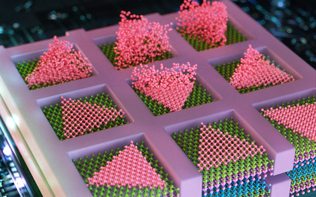
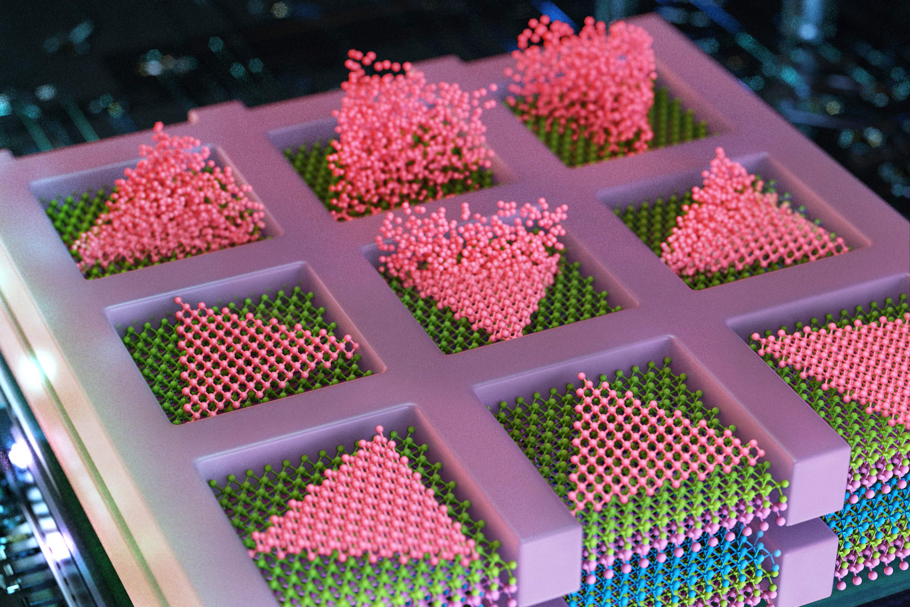
In 2023, the Goldbody Team reported that they developed a method for growing high-quality semiconductor materials on an amorphous surface, similar to various terrain of semiconductor circuits on finished chips. The material they grow is a 2D material called the transition metal di-salt element (TMD), considered a promising successor to silicon, used to make smaller, high-performance transistors. Such 2D materials can maintain their semiconductor properties even on the scale of a single atom, while silicon’s performance drops sharply.
In their previous work, the team used amorphous coatings on silicon wafers as well as TMDs on existing TMDs. To encourage atoms to arrange themselves into high-quality single crystal forms rather than in units of random polycrystalline diseases, Kim and his colleagues first covered silicon wafers in very thin films, or “masks” of silica, in tiny openings or pocketing or pockets or pockets. They then flowed the atoms’ gas onto the mask and found that the atoms were pocketed with “seeds”. The pocket restricts the seeds to grow in a conventional single crystal pattern.
But at that time, the method only worked around 900 degrees Celsius.
“You have to plant this single crystal material below 400 degrees Celsius, or the base circuit will be completely cooked and broken,” King said. “So our job is that we have to do similar techniques at temperatures below 400 degrees Celsius. The impact would be huge if we could.”
Establish
In their new work, King and his colleagues seek fine-tuning methods to plant monocrystalline 2D materials at a temperature low enough to retain any underlying circuitry. They found a surprisingly simple solution in metallurgy – the science and technology of metal production. When metallurgists pour molten metal into bad bacteria, the liquid slowly “nucleates” or forms grains, forming crystals that grow and merge into frequently patterned crystals that harden into solid form. Metallurgists have found that this nucleation is most likely to occur at the edge of a mold that is poured into liquid metal.
“It is well known that edge nucleation requires less energy and heat,” King said. “So we borrowed this concept from metallurgy and used it for future AI hardware.”
The team hopes to plant single crystal TMD on silicon wafers that have been made with transistor circuits. They first covered the circuit with a silica mask, just like they did before. They then deposited the TMD “seeds” at the edges of each mask’s pocket and found that these edge seeds grew into single crystal material at temperatures as low as 380 degrees Celsius, which required higher temperatures to form a higher temperature for single crystal material than the seeds that began to grow in the center.
Taking a step further, the researchers used a new approach to fabricating a multilayer chip with two alternating layers of different TMDs – Motybdenum disulfide, a promising material for making N-type transistors; and Dungsten diselenide, which has the potential to be made into P-type transistors. Both P- and N-type transistors are electronic building blocks that perform any logic operation. The team was able to grow both materials directly on top of each other in single crystal form without any intermediate silicon wafers. King said the method would effectively double the density of the chip’s semiconductor elements, especially metal oxide semiconductors (CMOS), which is the basic building block of modern logic circuits.
“The products we implement in our technology are not only 3D logic chips, but 3D memory and their combinations,” Kim said. “With our overall 3D approach based on growth, you can grow dozens to hundreds of logic and memory layers, and they will be able to communicate well with each other.”
“The traditional 3D chips are made from silicon wafers drilled with lenses, a process that limits the number of stacked layers, vertical alignment resolution and yield,” first author Kiseok Kim added. “We solve all these problems at once based on growth.”
To further commercialize its stackable chip design, Kim recently departed from a company called FS2 (Future Semiconductor 2D Materials).
“So far, we have demonstrated a concept in small device arrays,” he said. “The next step is to scale up to show professional AI chip operations.”
Samsung Advanced Technical College and the U.S. Air Force Office of Scientific Research support the study in part.